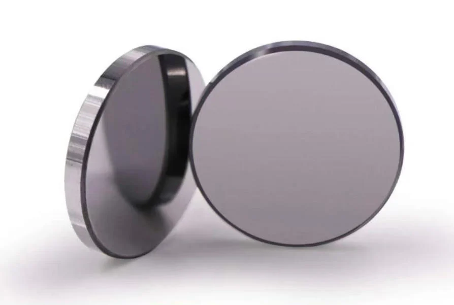
355nm 1064nm 10.6μm High Laser Damage Threshold Coating Fused Silica Substrate
Asin Optics customs and manufactures high LIDT super polished fused Silica Laser Optics for high power lasers. We are specialized in sub-nanometer roughness Rq≤0.2nm, 10-5 scratch-dig, and precision coatings. Inquire now for your custom specification
355nm 1064nm 10.6μm High Laser Damage Threshold Coating Fused Silica Substrate Product Discription
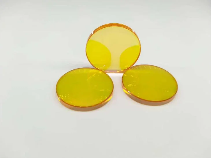
In high-power laser systems, the laser damage threshold of optical components determines the system’s stability and service life. Asin Optics offers high-laser-damage-threshold coatings for a variety of wavelengths. Using fused silica substrates and advanced high-damage-threshold dielectric coating designs, we cover the ultraviolet, near-infrared, and far-infrared wavelength ranges. Specifically optimized for the 355 nm, 1064 nm, and 10.6 μm. We provide a wide range of high-power laser window plates, protective lenses, and beam combining mirrors for the laser processing and research industries, ensuring these products maintain exceptional performance even in high-power laser environments.
Our Cure High Laser Damage Threshold Coating Technical Advantages
- Our high laser-induced damage threshold (LIDT) coating designs can be optimized for single wavelengths or for simultaneous operation across multiple wavelengths—such as 355 nm, 1064 nm, and 10.6 µm.
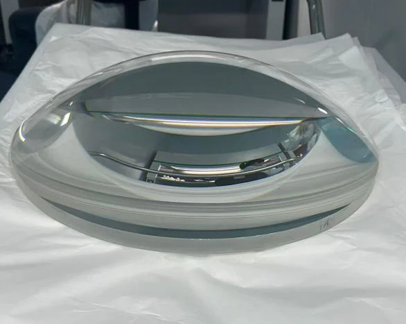
- We utilize high-purity imported fused silica, characterized by an extremely low coefficient of thermal expansion and exceptional stability. Even after absorbing laser energy, the optical surface maintains a transmitted wavefront accuracy of better than λ/15, a parallelism of ≤ 2 arcseconds, and a surface figure accuracy of RMS < λ/60. This capability effectively mitigates thermal lensing effects and wavefront distortion.
- Based on our clients’ specific requirements, we offer a comprehensive range of coatings, including anti-reflective (AR) coatings, high-reflective (HR) coatings, beam-splitting coatings, and partial-reflective coatings.
- Employing advanced chemical-mechanical polishing (CMP) and magnetorheological finishing (MRF) processes, we guarantee a surface roughness of Rq ≤ 0.2 nm. This minimizes scattering to the greatest extent possible, ensuring ultra-low insertion loss even in kilowatt-class laser systems.
- Leveraging our expertise in ion-beam sputtering (IBS) and ion-assisted electron-beam evaporation technologies, we maintain strict control over reflectivity: R < 0.1% at a wavelength of 1064 nm, and R < 0.5% at 10.6 µm.
- We possess ultra-large aperture coating capabilities, capable of processing optical components with diameters ranging from 400 mm to 1200 mm.
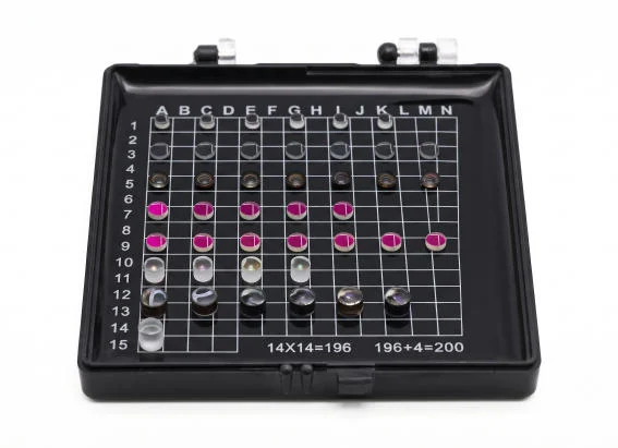
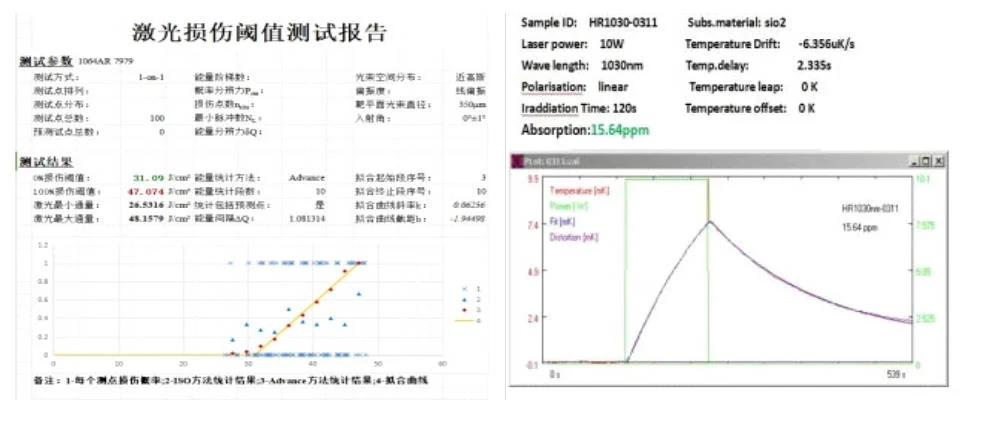
high Laser Damage Threshold Coating Testing Report
Custom and Manufacturing Capability Of High Laser Damage Threshold Coating
High LIDT Fused Silica & ZnSe Laser Optics Applications
-
High-Power Fiber and Nd:YAG Laser Systems
During welding and cutting processes, multi-kilowatt 1064 nm lasers generate metal spatter, intense thermal radiation, and strong scattered light. Conventional optical lenses—characterized by high surface roughness and high coating absorption—are prone to thermal heating, thermal lensing effects, and coating damage; furthermore, any adhering spatter is extremely difficult to clean. For the focusing lenses and protective windows within cutting and welding heads, we utilize ultra-smooth substrates with a surface roughness of Rq ≤ 0.2 nm, paired with Ion-Beam Sputtering (IBS) coatings that exhibit a residual reflectance of R < 0.1% at 1064 nm. This design effectively suppresses thermal lensing effects, thereby ensuring consistent weld penetration depth and cut kerf width over extended periods of operation.
-
Semiconductor Metrology
Semiconductor inspection equipment is acutely sensitive to wavefront distortion and light scattering. Ordinary optical windows and mirrors with significant surface figure errors (RMS > λ/20) can introduce spurious signals, while surface roughness exceeding 0.3 nm generates stray light that can drown out the signals of minute defects. When deployed as windows, beam splitters, or mirrors within inspection optical paths, our components feature a surface figure precision of RMS < λ/60 (approximately 10 nm at 633 nm) and a parallelism of ≤ 2 arcseconds, ensuring nearly ideal transmitted and reflected wavefronts. This capability reduces the minimum detectable defect size from tens of nanometers down to the sub-10 nm range, thereby meeting the rigorous demands of advanced semiconductor fabrication processes (such as 3 nm and 5 nm nodes).
-
Large-Scale Laser Astronomical Observation
Large-aperture optical components—such as those made from fused silica reaching diameters of up to φ1200 mm—require exceptionally low wavefront error and minimal light scattering. Simultaneously, they must demonstrate robust thermal stability to withstand the extreme conditions of space environments or the thermal cycling (heating and cooling) inherent to nighttime astronomical observations. These products serve as laser guide star launch windows in astronomical telescopes or as transmit/receive isolation windows in space-based laser communication terminals. By leveraging our ultra-large-scale fabrication capabilities to produce components with the exact required aperture, and by combining this with sub-nanometer surface roughness, we effectively minimize Rayleigh scattering. This approach significantly enhances the signal-to-noise ratio for the detection of faint signals while simultaneously reducing background light noise.
-
High-Power Continuous-Wave (CW) and Pulsed Laser Cutting & Welding
Kilowatt-class lasers generate extremely intense thermal effects and significant light scattering. Conventional optical components are susceptible to damage caused by surface absorption or electric field enhancement, while thermal lensing effects can lead to focal point drift. Optical components featuring a high laser-induced damage threshold (LIDT) serve as focusing lenses, mirrors, or protective windows within laser processing heads. By utilizing ultra-low surface roughness (Rq ≤ 0.2 nm) to minimize scattering, employing high-LIDT coatings (R < 0.1% at 1064 nm) to suppress film absorption, and ensuring instrument-grade surface figure accuracy, these components effectively preserve beam quality. This approach significantly extends the operational lifespan of the optical elements.