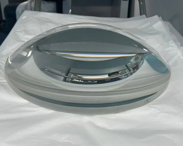
Large Aperture Spherical Lens for Photomask Exposure
Asin Optics is specialized in customing and manufacturing large aperture spherical lens for photomask exposure. We also apply high LIDT 365nm, 405nm, 248nm, 193nm thin film coating to the lens. We understand the confidentiality of semiconductor semiconductor/FPD projects. Contact us for secure NDA-backed custom design reviews
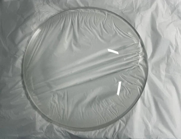
Large Aperture Spherical Lens for Photomask Exposure Product Discription
In semiconductor lithography, high-precision photomask exposure, and laser direct-writing systems, the core lenses within projection objectives and illumination optical systems directly determine exposure uniformity. Unlike standard imaging lenses, photomask exposure lenses must operate at specific wavelengths (typically i-line 365nm, h-line 405nm, g-line 436nm, or DUV 248nm/193nm) while simultaneously delivering large apertures (Φ50mm – Φ300mm+), minimal wavefront aberration (λ/10 – λ/20), and exceptional transmission uniformity; even minute surface figure errors can lead to distortion in lithographic patterns.
The large-aperture spherical lenses manufactured by Asin Optics are high-precision optical components specifically designed for photomask exposure equipment, serving as critical elements in projection objectives, illumination optics, or 1:1 imaging systems. Leveraging proprietary tooling for coating extra-large apertures and advanced uniformity control processes, we utilize imported optical materials with ultra-low thermal expansion coefficients. Combined with our proprietary deep-UV anti-reflective coatings—which feature high laser-induced damage thresholds—these lenses ensure high-resolution imaging and uniform illumination delivery for photomask exposure systems.
Our Large Diameter Spherical Lens for Photomask Exposure Core Advantage
- We offer large-aperture spherical lenses for photomask exposure applications with wavefront errors better than λ/10.
We utilize ultra-high-purity synthetic fused silica from top-tier global brands such as Corning and Heraeus. This material is free of internal bubbles and striae, offers exceptional transmittance in the deep-UV range, and supports surface figure accuracy of up to λ/20, while effectively resisting long-term UV-induced degradation (solarization). - We provide customized vacuum ion-assisted deposition (IAD) coating services for UV wavelengths including 365nm, 405nm, and 248nm, achieving single-surface reflectance of R < 0.25%. Additionally, our specialized high-laser-damage-threshold coatings prevent film delamination and damage caused by high-energy concentration.
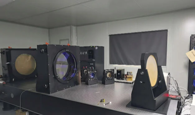
- Every large-aperture exposure lens undergoes rigorous inspection using our large-aperture laser interferometers (ZYGO) and ultra-high-precision profilometers prior to shipment. Each unit is supplied with a comprehensive color wavefront map and a Certificate of Conformance (CoC), ensuring the delivered product aligns perfectly with your optical design specifications.
Photomask Exposure Lens Custom Process
- Upon receipt of technical specifications or drawings, we evaluate parameters such as wavelength, aperture, focal length, and wavefront error.
- We internally determine the appropriate materials and coating solutions based on the client’s specific operating wavelength and power levels.
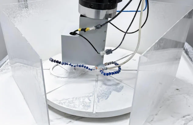
- Grinding and polishing are performed in a temperature- and humidity-controlled workshop to ensure surface uniformity.
- We issue comprehensive inspection reports using equipment such as large-aperture Zygo laser interferometers, spectrophotometers, and focal length meters.
- We ensure safe, global delivery.
Asin Custom Capability Of Lithography Spherical Optical Lens
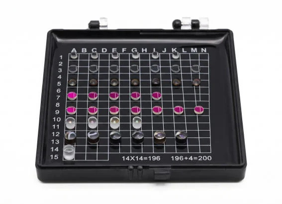
Large aperture lens for semiconductor exposure Metrology
Photomask Exposure Equipment
Photomask exposure is the core process of transferring design patterns onto a mask—either at a 1:1 scale or via magnification—requiring diffraction-limited resolution in the i-line (365 nm) wavelength range. Standard lenses struggle to simultaneously achieve large apertures, high transmission, and minimal wavefront error; we precision-machine high-purity fused silica into large-aperture lenses with surface figure accuracy of λ/10, serving as core components for projection objectives or 1:1 imaging lenses. These lenses undergo CNC polishing to achieve a surface figure PV value better than λ/10 and a surface roughness below 0.5 nm. They are also coated with broadband anti-reflective coatings optimized for 365 nm. A single i-line exposure spherical lens can control full-aperture wavefront error to within λ/10 or even λ/15, ensuring pattern fidelity without distortion or line breakage.
Semiconductor Stepper and Scanner Alignment Optics
Alignment systems must precisely overlay the alignment marks on the mask and the wafer with nanometer-level accuracy prior to exposure. Alignment optical paths typically operate at 365 nm or across a broadband UV spectrum, requiring large-aperture lenses to capture diffracted light signals with minimal aberration. Our large-aperture UV imaging and collimating lenses are integrated into off-axis or on-axis alignment systems. They ensure high-quality imaging of mark patterns or diffracted beams onto detectors, thereby enhancing alignment precision and overlay yields.
PCB Direct Imaging and Laser Exposure
PCB direct imaging equipment exposes patterns directly onto dry film or solder masks using spatial light modulators (such as DMDs) or laser beam scanning, eliminating the need for photomasks. To achieve high throughput and fine-line resolution, the system requires a large-area, highly uniform UV illumination field. Large-aperture UV collimating lenses are responsible for collimating and shaping UV laser or LED beams to cover the entire work surface; these lenses ensure the exposure beam maintains excellent parallelism across the large area, minimizing line-width variations between the edges and the center.