Large Aperture Optical Components Up to 2000mm Thin Film Coating
Asin customs and manufactures meter-scale optical coating up to 2 meters in China. We can ultilize low stress coating and high uniformity coating for large thin substrates. Contact us for your large optics CAD Drawing for a Feasibility Evaluation.
Precision Large-Aperture Optical Coating Services Up to 2000mm
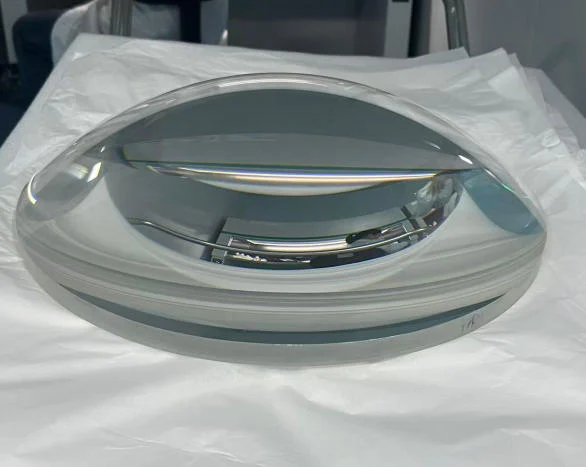
Large-aperture optical components are critical to the overall performance of a system. As component size increases, challenges arise in areas such as coating difficulty, uniformity, wavefront distortion, laser damage threshold, and environmental stability. Asin Optics possesses the capability to coat and process large-aperture optical components with diameters up to 2000 mm. We can process both circular and irregular substrates, with substrate materials including, but not limited to, fused silica, glass-ceramic glass, silicon carbide, monocrystalline silicon, sapphire, calcium fluoride, and zinc selenide. Using custom-designed fixtures, we can successfully process even extremely large, lightweight mirrors or high-value crystals.
Different Thin Film Coating Process We Use
We use two coating methods:
- Electron Beam Evaporation and Ion-Assisted Deposition: This method is suitable for various oxide and fluoride coating systems spanning the UV to IR spectrum.
- Ion Beam Sputtering (IBS): The advantages of ion beam sputtering include low loss and high stability, making it particularly suitable for applications requiring low absorption and high damage thresholds.
Furthermore, by integrating a multi-zone independent correction mask system with real-time optical monitoring and crystal control dual feedback, we are able to maintain coating thickness uniformity within ±1% across the entire 2000 mm diameter, achieving excellent spectral consistency
Custom Capability Of Thin Film Coating Design
Our design and process teams specialize in the development of thin-film coatings spanning an exceptionally broad spectral range—from the deep ultraviolet (190 nm) to the long-wave infrared (15 μm). Common coating types include:
- High-Performance Anti-Reflection (AR) Coatings: Featuring residual reflectance as low as <0.1%, supporting wide-angle and broadband designs.
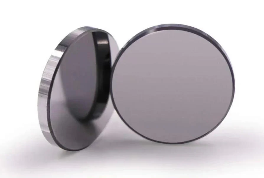
- High-Reflection (HR) Coatings: Achieving reflectance levels exceeding 99.9%.
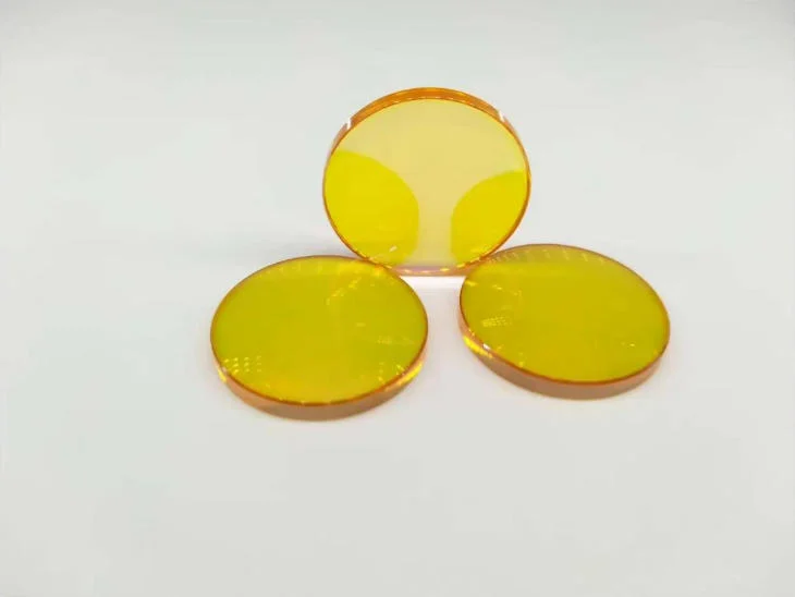
- Dichroic Mirrors / Beam Splitters: Characterized by steep transition bands and precise splitting ratios (e.g., 50:50, 30:70).
- Broadband Metal-Enhanced Reflective Coatings: Silver-, gold-, and aluminum-enhanced films optimized for high reflectance.
- ITO Transparent Conductive Coatings and Diamond-Like Carbon (DLC) Protective Coatings.
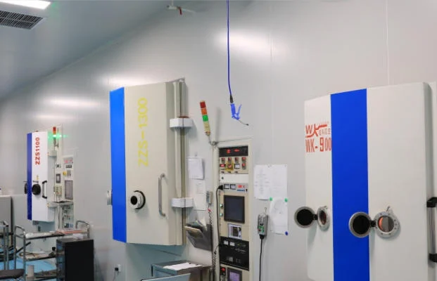
Capabilities & Hardware: Large-Scale Vacuum Chambers
To accommodate optical components with diameters of up to two meters, we have installed a massive vacuum coating system specifically designed for oversized components.
- The chamber’s inner diameter is optimized for 2000 mm components, capable of accommodating circular substrates with a maximum diameter of 2000 mm, or rectangular and irregularly shaped components with a diagonal length of up to 2000 mm (e.g., 1800 mm × 1200 mm).
- The loading platform can accommodate components weighing up to 500 kg, making it suitable for handling both heavy mirrors and lightweight optical assemblies. The fixtures support virtually all optical materials, including fused silica, microcrystalline glass, ULE, silicon carbide, monocrystalline silicon, sapphire, calcium fluoride, and zinc selenide.
Solving Key Technical Challenges in Large Optics Coating
Challenge 1: Extreme Film Thickness Uniformity Across a 2000 mm Full Aperture
Maintaining spectral consistency over a large surface area presents a formidable challenge. By leveraging multi-zone mask correction algorithms and a real-time dual-feedback closed-loop system (combining optical and crystal monitoring), we consistently maintain film thickness uniformity within ±1%.
Challenge 2: Wavefront Distortion Control
Through the implementation of low-stress coating designs, precise deposition parameter tuning, and chamber temperature gradient management, we limit coating-induced wavefront errors (in both transmission and reflection) to less than λ/10 RMS. Specialized optimization processes can achieve levels as low as λ/20 (at 633 nm), thereby guaranteeing the imaging quality of large-aperture optical systems.
Challenge 3: Ensuring Laser Damage Thresholds for Large-Scale Components
The probability of defects rises exponentially as surface area increases. We have developed low-absorption, low-defect deposition processes—combined with deep substrate cleaning and post-coating standing wave field optimization—to ensure the reliability of large-aperture, high-energy laser components.
Challenge 4: Environmental Stability
We strictly adhere to standards such as MIL-C-48497 and MIL-PRF-13830. Through rigorous testing—including thermal cycling from -55°C to +85°C, prolonged exposure to high humidity and heat, adhesion pull-tests, and salt spray exposure—we guarantee that our coatings remain free from cracking, delamination, or spectral drift under varying humidity conditions.
Metrology and Inspection for Large Diameter Components
large scale optical coating service
meter-scale optical coating
large diameter mirror coating
oating for 500mm mirrors
800nm coating on 1-meter substrate
large optics vacuum chamber coating
large SiC mirror coating
large aperture zero-dur reflection coating
astronomical telescope mirror coating supplier
coating thickness uniformity large optics